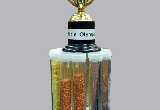
I co-instruct and coordinate an undergraduate materials and nanoscience (MNS) lab at the University of Waterloo. One experiment in 2nd year consistently stands out as my students’ favourite, and it involves the synthesis and characterization of “capped” cadmium selenide (CdSe) “quantum dots” (QDs). Quantum dots are a type of nanoparticle. Here a nanoparticle is defined as a particle with a diameter of 1 to 100 nanometres. I would like to share this lab with chemistry teachers who might be wondering, “Have undergrad chem labs changed since I graduated?”
What is a capped quantum dot?
A capped QD is a nanocrystal (~2 to 20 nm in diameter) composed of a material that acts as a semiconductor in the bulk (e.g., in macroscopic quantities). The term “capped” arises from the fact that the surface of each QD is functionalized with organic ligands such as trioctylphosphine and/or hexadecylamine, to name a couple of examples. Capping QDs with unique combinations of organic ligands facilitates their dissolution in a range of solvents that would normally not dissolve inorganic substances like CdSe.
In bulk CdSe, the “ground state” (i.e., lowest energy) valence electrons can have energy values that exist within a particular energy range, referred to as the “valence band”. This is analogous for “excited state” (i.e., having energies above the ground state) electrons, which can have energy values that exist within a particular energy range, referred to as the “conduction band”. In each case, the energy bands form a continuum of possible energy values. The valence and conduction bands are energetically separated by a region in which no electronic energy states exist called the “band gap” (Ebg). In order to excite electrons from the valence band to the conduction band, using light, the energies of the irradiated photons must be above the energy of the band gap. (Refer to Fig. 1.)
In contrast to bulk CdSe in which electrons are more delocalized (i.e., spread out) throughout a relatively large volume, in CdSe QDs, electrons are confined to a much smaller volume because of the small size of the QD. The observed consequence of this so-called “quantum confinement” effect is that the allowed electron energies in the valence and conduction bands become “quantized” (i.e., discrete) as opposed to continuous. As the size of the CdSe QDs decreases the energy levels become more discrete and the band gap increases (see Fig. 1). The size of the band gap can be “tuned” to a desired value determined only by the size of the QD and not by the type of material used to make the QD. (Refer to Fig. 1). The wonderful thing about QDs is that one is able to control their optical properties by controlling their size.
It is important to mention that cadmium, and all forms of its compounds, are highly toxic. In this case, it is imperative that all work be done within a high-quality fume hood or, better still, a glove box. The use of personal protective equipment such as high-quality nitrile gloves and eye protection is mandatory. Finally, because cadmium is a heavy metal, all of its compounds must be disposed of using an appropriate environmental protocol. Elemental selenium is also highly toxic and should be handled in the same manner as cadmium compounds. We have been working in a fume hood but our Chem Department has just purchased a glove box for this undergraduate lab.

Fig. 1. A schematic representation that shows how the transition from the bulk to the nanoscale changes the electronic energy levels and band gap (Ebg) in CdSe. Notice the compound is the same; it is the particle size that changes.
The procedure used in my lab is adapted from the procedure reported by Williams et al.1 (Refer to Fig. 2). Here I provide only a brief summary; however, if you are interested in the complete procedure, I am happy to share it. To enable the removal of aliquots of the reaction mixture at different time intervals while having the reaction take place under nitrogen, a 100 mL three neck round bottom flask with a stir bar is used — vigourous stirring is required throughout. The starting material is 40.0 mg of cadmium oxide, 1.55 g of trioctylphosphine oxide and 3.65 g of hexadecylamine — notice the small amount of CdO required. After this mixture is heated to 270 °C (± 5 °C), 0.5 g of decylphosphonic acid is added. When the mixture becomes optically transparent, the temperature is reduced to 250 °C (± 5 °C) and 40.0 mg of selenium (dissolved in 2.5 mL of trioctylphosphine) is added.
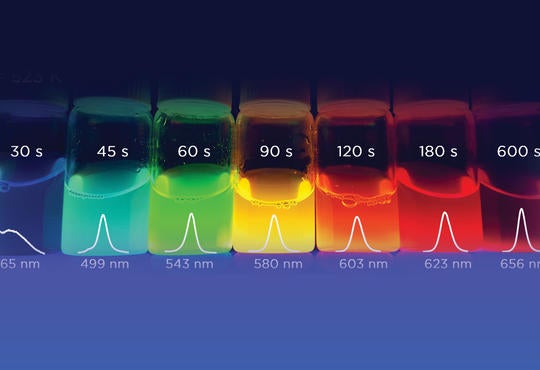
The formation of CdSe QDs begins immediately; aliquots (~1.0 to 1.5 mL) of the reaction mixture are removed using a glass Pasteur pipet (one for each aliquot) at intervals of: 30, 45, 60, 90, 120, 180 and 600 seconds. Each aliquot is placed in a 20 mL glass scintillation vial. Lastly, the capped CdSe QDs are dissolved in 10 mL of toluene. This is why CdSe QD are capped — to have the quantum dots dissolved in this solvent. Once dissolved, the solutions can be irradiated with a standard black light (i.e., a long wave ultraviolet light source) to produce beautifully fluorescing solutions like those shown in Fig. 3. The wavelengths of the colours observed during fluorescence can be determined quantitatively using a photoluminescence spectrophotometer (i.e., “fluorometer”).
Why do QDs collected at different reaction times fluoresce different colours?

Fig. 2. A schematic representation of the apparatus used for the capped CdSe QD synthesis described here.
Fig. 3 clearly shows that the solutions of QDs collected at different reaction times fluoresce over a range colours across the visible spectrum (i.e., wavelengths from ~400 to 750 nm). The observation can be easily rationalized by considering Fig. 1, but before doing so it is instructive to briefly describe the process of fluorescence. Fluorescence involves the excitation of an electron from the ground state to a higher energy excited state by the absorption of a photon. In the excited state, the electron can transfer some energy through a variety of non-radiative processes, but mainly through molecular vibrations. Molecular vibrations happen very quickly, on the order of 10−12 s, whereas the entire fluorescence process takes ~10−9 to 10−5 s.2 Ultimately the electron loses the remaining excess energy by the emission of a photon. The photon emitted by the excited electron is lower in energy than the photon that was originally absorbed because some energy was transferred in the excited state. In other words, the wavelength of the lower energy emitted photon is longer than the wavelength of the higher energy absorbed photon (Note that the energy of photon, Ephoton, is related to wavelength, l, by Ephoton = hc/l, where h and c are Planck’s constant and the speed of light in a vacuum, respectively).

Fig. 3. Irradiation with a black light causes solutions of capped CdSe QDs to strongly fluoresce. Each time shown represents the time at which the aliquot was removed during the reaction. The size of the CdSe QD increases with reaction time and the band gap decreases, resulting in fluorescence in emissions of longer wavelengths (shift towards the visible red). The energy of the photon is the energy of Ebg.
 Fig. 4. A plot of fluorescence emission as a function of wavelength for capped CdSe QDs obtained at different reaction times (in seconds). Note that the sample obtained at 30 s had a very low concentration of QDs, resulting in a “noisy” spectrum because of a lack of signal intensity.
Consider Fig. 1: As the size of the QDs increases with reaction time, the size of the band gap decreases. Recall that the band gap, Ebg, represents the difference in energy between the electronic ground (i.e., valence band) and excited (i.e., conduction band) states. Therefore, smaller QDs, obtained at short reaction times, have relatively large band gaps and their fluorescence results in the emission of shorter (i.e., shift toward the visible blue) wavelengths of light. Larger QDs, obtained at longer reaction times, have relatively smaller band gaps and their fluorescence results in the emission of longer (i.e., shift toward the visible red) wavelengths of light. Fluorescence emission spectra for all of the samples in Fig. 3 are shown in Fig. 4. The wavelength of the maximum intensity of a fluorescence emission plot can be associated with the observed colour. This basically shows students the colour emitted from quantum dots is directly related to its size — which we can control and measure.
What might QDs be used for?
The commercial use of QDs for their optical properties is desirable because they have tunable and narrow emission wavelengths leading to the emission of very “pure” coloured light; they exhibit highly-efficient fluorescence emission (“quantum yield”); and finally, the ranges of excitation wavelengths that lead to fluorescence emission are very broad.
The commercial application of CdSe QDs is limited by the environmental toxicity of cadmium; however, CdSe QDs find extensive applications in fundamental research.3-6 Additionally, QDs can be made from compounds that are free of heavy toxic metals (e.g., Cd, Pb, etc.); compounds such as ZnAgInS, CuInS, ZnS3 and InP,7 to name a few.
Currently, QDs are being used in the development of devices such as solar cells, field-effect transistors and light emitting diodes.7 Devices constructed from quantum dots can be made to be physically flexible and at low cost. For example, Samsung’s current flagship QLEDTM televisions use InP/ZnS QDs to produce beautiful, high-contrast/resolution pictures.7
Ask your students if they have heard of quantum dot displays, given most are interested in their own devices and high tech screens. You can use this as an opportunity to discuss nanochemistry and several curriculum topics, such as metallic compounds, solubility based on polarity, energy of a photon and energy states.
References
- B.M. Hutchins, T.T. Morgan, M.G. Ucak-Astarlioglu and M.E. Williams, Journal of Chemical Education, 2007, 84, page 1301.
- D.A. Skoog, F.J. Holler and T.A. Nieman, Principles of Instrumental Analysis; 5th edition.; Nelson Thomas Learning; 1120 Birchmount Road, Toronto ON, M1K 5G4, Canada, 2003.
- M.J. Lee, J. Lee, H. Yang and K. Hong, Current Applied Physics, 2017, 17, page 880.
- R. Nadler and J.F. Sanz, Journal of Physical Chemistry A, 2015, 119, page 1218.
- K. Kaviyarasu, K. Kanimozhi, N. Matinise, C.M. Magdalane, G.T. Mola, J. Kennedy, M. Maaza, Materials Science and Engineering C, 2017, 76, page 1012.
- S. Hooshmand and Z. Es’haghi, Analytical Chimica Acta, 2017, 972, page 28.
- C.R. Kagan, E. Lifshitz, E.H. Sargent and D.C. Talapin, Science 2016, 353, page 885.